Module functions
Modules are library components that operate with the MCU’s internal peripherals. Every module has its own namespace according to the module name. For example, Power Manager has module namespace of pm_, Realtime Counter falls under the rtc_ namespace, etc. To use the module just include its header file. These header files are also named after the module name. So, for example, to include and use functions that operate with the Power Manager include <aery32/pm.h>.
Naming convention and the calling order
The common calling order for modules is the following: 1) initialize, 2) do some extra setuping and after then 3) enable the module. In pseudo code it looks like this
module_init();
module_setup_something();
module_enable();
The init function may also look like module_init_something(), for example, the SPI can be initialized as a master or slave, so the naming convention declares two init functions for SPI module: spi_init_master() and spi_init_slave().
If the module has been disabled, by using module_disable() function, it can be re-enabled without calling the init or setup functions. Most of the modules can also be reinitialized without disabling it before. For example, general clock frequencies can be changed by just calling the init function again – this is also the quickest way to change the frequency
pm_init_gclk(GCLK0, GCLK_SOURCE_PLL1, 1);
pm_enable_gclk(GCLK0);

/* Change the frequency divider */
pm_init_gclk(GCLK0, GCLK_SOURCE_PLL1, 6);
If you have read through the MCU datasheet, you may wonder why you cannot set all the possible settings with the initialization and setup functions. This is because these functions set sane default values for those properties. These default values should work for 80-90% of use cases. However, sometimes you may have to fine tune these properties to match your needs. This can be done by bitbanging the module registers after you have called the init or setup function. For example, the SPI chip select baudrate is hard coded to MCK/255 within the spi_setup_npcs() function. To make SPI bus faster you can bitbang the SCRB bit within CSRn register, where n is the NPCS number.
spi_setup_npcs(spi0, 0, SPI_MODE1, 16);
spi0->CSR0.scbr = 32; /* SPI baudrate for the CS0 is now MCK/32 */
Note
Modules never take care of pin initialization, except GPIO module that’s for this specific purpose. So, for example, when initializing SPI you have to take care of pin configuration!
#define SPI0_GPIO_MASK ((1 << 10) | (1 << 11) | (1 << 12) | (1 << 13))
gpio_init_pins(porta, SPI0_GPIO_MASK, GPIO_FUNCTION_A);
Global variables and error handling
Every module declares global shortcut variables to the main registers of the module. For example, the GPIO module declares porta, b and c global pointers to the MCU ports by default. Otherwise, you should have been more verbose and use &AVR32_GPIO.port[0], &AVR32_GPIO.port[1] and &AVR32_GPIO.port[2], respectively. Similarly, pll0 and pll1 declared in PM module provide quick access to MCU PLL registers etc.
Hint
As porta, b and c are pointers to the GPIO port, you can access its registers with arrow operator, for example, instead of using function gpio_toggle_pin(AVR32_PIN_PC04) you could have written portc->ovrt = (1 << 4); This is also way how you can set/unset/read/toggle multiple pins at once. Refer to the UC3A0/1 datasheet pages 175–177 for GPIO Register Map.
Error handling
All module functions will return -1 on general error. This will happen most probably because of invalid parameter values. Greater nagative return values have a specific meaning and a macro definition in the module’s header file. For example, flashc_save_page() of Flash Controller may return -2 and -3, which have been defined with E prefixed names EFLASH_PAGE_LOCKED and EFLASH_PROG_ERR, respectively.
Analog-to-digital conversion, #include <aery32/adc.h>
UC3A0/1 microcontrollers have eight 10-bit analog-to-digital converters. The maximum ADC clock frequency for the 10-bit precision is 5 MHz. For 8-bit precision it is 8 MHz. This frequency is related to the frequency of the Peripheral Bus A (PBA).
adc_init(
    7,    /* prescal, adclk = pba_clk / (2 * (prescal+1)) */
    true, /* hires, 10-bit (false would be 8-bit) */
    0,    /* shtim, sample and hold time = (shtim + 1) / adclk */
    0     /* startup, startup time = (startup + 1) * 8 / adclk */
);
The initialization statement given above, uses the prescaler value 7, so if the PBA clock was 66 MHz, the ADC clock would be 4.125 MHz. After initialization, you have to enable the channels that you like to use for the conversion. For example, to enable channel three call
adc_enable(1 << 3);
Now you can start the conversion. Be sure to wait that the conversion is ready before reading the conversion value.
uint16_t result;

adc_start_cnv();
while (adc_isbusy(1 << 3));
result = adc_read_cnv(3);
If you only want to read the latest conversion, whatever was the channel, you can omit the channel mask for the busy function and read the conversion with another function like this
while (adc_isbusy());
result = adc_read_lastcnv();
ADC hardware triggers
To setup the ADC hardware trigger, call adc_setup_trigger() after init
adc_setup_trigger(EXTERNAL_TRG);
Other possible trigger sources, that can be used for example with the Timer/Counter module, are
|
|
|
Note
You always have to call adc_start_cnv() individually for every started conversion. If you suspect that your conversions may have overrun, you can check this with the adc_has_overrun(chamask) function. If you omit the channel mask input param, all the channels will be checked, being essentially the same than calling adc_has_overrun(0xff).
Flash Controller, #include <aery32/flashc.h>
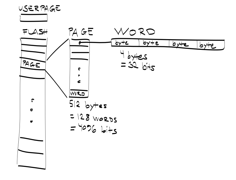
Flash Controller provides low-level access to the chip’s internal flash memory, whose structure has been sketched in the figure above. The init function of the Flash Controller sets the flash wait state (zero or one, FLASH_0WS or FLASH_1WS, respectively). The last param of the init function enables/disables the sense amplifiers of flash controller.
flashc_init(FLASH_1WS, true);
Warning
Setting up the correct flash wait state is extremely important! Note that this has to be set correctly even if the flash read and write operations, described below, are not used. If CPU clock speed is higher than 33 MHz you have to use one wait state for flash. Otherwise you can use zero wait state.
Warning
The uploaded program is also stored into the flash, so it is possible to overwrite it by using the Flash controller. The best practice for flash programming, is starting from the top. FLASH_LAST_PAGE macro definition gives the number of the last page in the flash. For 128 KB flash this would be 255.
Warning
According to Atmel UC3A1’s internal flash supports approximately 100,000 write cycles and it has 15-year data retention. However, you can easily make a for-loop with 100,000 writes to the same spot of flash and destroy your chip in a second. So be careful!
Read and write operations
Flash memory is accessed via pages that are 512 bytes long. This means that you have to make sure that your page buffer is large enough to read and write pages, like this
#include <cstring>

char buf[512];
flashc_read_page(FLASH_LAST_PAGE, buf); /* Read the last page to separate page buffer */
strcpy(buf, "foo");                     /* Save string "foo" to page buffer */
flashc_save_page(FLASH_LAST_PAGE, buf); /* Write page buffer back to flash */
You can also read and write values with different types as long as the page buffer size is that 512 bytes. For example like this
extern "C" #include <inttypes.h>

uint16_t buf16[256];
uint32_t buf32[128];
Page locking
The flash page can be locked to prevent the write and erase sequences. To lock the first page (page number 0), call
flashc_lock_page(0);
Locking is performed on a per-region basis, so the above statement does not lock only page zero, but all pages within the region. There are 16 pages per region so the above command locks also pages 1-15.
To unlock the page, call
flashc_unlock_page(0);
You can also use, flashc_lock_page_region() and flashc_unlock_page_region(). to lock and unlock pages by region. Furthermore, there is a function to check if the page is empty
flashc_isempty(0);
User page
The User page is an additional page, outside the regular flash array, that can be used to store various data, like calibration data and serial numbers. This page is not erased by regular chip erase. The User page can only be read and write by proprietary commands, which are
uint8_t buf[512];
flashc_read_userpage(buf);
and
flashc_save_userpage(buf);
To check whether the user page is empty or not call
flashc_userpage_isempty();
General purpose fuse bits
You can read all 32 fuse bits into 32 bit variable by using the following command
uint32_t fusebits;
fusebits = flashc_read_fusebits();
To write one bit true or false use this:
flashc_write_fusebit(uint16_t fusebit, bool value);
You can also write fuse bits by a byte at a time, like this
flashc_write_fusebyte(0, 0xff);
flashc_write_fusebyte(1, 0xff);
flashc_write_fusebyte(2, 0xff);
flashc_write_fusebyte(3, 0xff);
Now all fuse bits are written to 1. The first parameter is the byte address that can be 0-3 in a 32-bit word and the second one is the byte value.
General Periheral Input/Output, #include <aery32/gpio.h>
To initialize any pin to be output high, there is a oneliner which can be used
gpio_init_pin(AVR32_PIN_PC04, GPIO_OUTPUT|GPIO_HIGH);
The first argument is the GPIO pin number and the second one is for options. For 100 pin Atmel AVR32UC3, the GPIO pin number is a decimal number from 0 to 69. Fortunately, you do not have to remember which number represent what port and pin. Instead you can use predefined aliases as it was done above with the pin PC04 (5th pin in port C if the PC00 is the 1st).
The available pin init options are:
|
|
|
These options can be combined with the pipe operator (boolean OR) to carry out several commands at once. Without this feature the above oneliner should be written with two lines of code:
gpio_init_pin(AVR32_PIN_PC04, GPIO_OUTPUT);
gpio_set_pin_high(AVR32_PIN_PC04);
Well now you also know how to set pin high, so you may guess that the following function sets it low
gpio_set_pin_low(AVR32_PIN_PC04);
and that the following toggles it
gpio_toggle_pin(AVR32_PIN_PC04);
and finally it should not be surprise that there is a read function too
state = gpio_read_pin(AVR32_PIN_PC04);
But before going any further, let’s quickly go through those pin init options. FUNCTION_A, B, C and D assing the pin to the specific peripheral function, see datasheet pages 45–48. INT_PIN_CHANGE, RAISING_EDGE and FALLING_EDGE enables interrupt events on the pin. Interrupts are trigged on pin change, at the rising edge or at falling edge, respectively. GPIO_PULLUP connects pin to the internal pull up resistor. GPIO_OPENDRAIN in turn makes the pin operate as an open drain mode. This mode is gererally used with pull up resistors to guarantee a high level on line when no driver is active. Lastly GPIO_GLITCH_FILTER activates the glitch filter and GPIO_HIZ makes the pin high impedance.
Usually you want to init several pins at once – not only one pin. This can be done for the pins that have the same port.
gpio_init_pins(porta, 0xffffffff, GPIO_INPUT); /* initializes all pins input */
The first argument is a pointer to the port register and the second one is the pin mask.
Note
Most of the combinations of GPIO init pin options do not make sense and have unknown consecuences.
Local GPIO bus
AVR32 includes so called local bus interface that connects its CPU to device-specific high-speed systems, such as floating-point units and fast GPIO ports. To enable local bus call
gpio_enable_localbus();
When enabled you have to operate with local GPIO registers. That is because, the convenience functions described above does not work local bus. To ease operating with local bus Aery32 GPIO module provides shortcuts to local ports by declaring lporta, b and c global pointers. Use these to read and write local port registers. For example, to toggle pin through local bus you can write
lporta->ovrt = (1 << 4);
Note
CPU clock has to match with PBB clock to make local bus functional
To disable local bus and go back to normal operation call
gpio_disable_localbus();
Interrupt Controller, #include <aery32/intc.h>
Before enabling interrupts define and register your interrupt service routine (ISR) functions. First write ISR function as you would do for any other functions
void myisr_for_group1(void) {
    /* do something */
}
Then register this function
intc_register_isrhandler(&myisr_for_group1, 1, 0);
Here the first parameter is a function pointer to your myisr_for_group1() function. The second parameter defines the which interrupt group calls this function and the last one tells the priority level.
Hint
Refer Table 12-3 (Interrupt Request Signal Map) in datasheet page 41 to see what peripheral belongs to which group. For example, RTC belongs to group 1.
When all the ISR functions have been declared it is time to initialize interrupts. Use the following init function to do all the magic
intc_init();
After initialization you can enable and disable interrupts globally by using these functions
intc_enable_globally();
intc_disable_globally();
Power Manager, #include <aery32/pm.h>
Power Manager controls integrated oscillators and PLLs among other power related things. By default the MCU runs on the internal RC oscillator (115 kHz). However, it’s often preferred to switch to the higher CPU clock frequency, so one of the first things what to do after the power up, is the initialization of oscillators. Aery32 Development Board has 12 MHz crystal oscillator connected to the OSC0. This can be started as
pm_start_osc(
    0,               /* oscillator number */
    OSC_MODE_GAIN3,  /* oscillator mode, see datasheet p.74 */
    OSC_STARTUP_36ms /* oscillator startup time */
);
pm_wait_osc_to_stabilize(0);
When the oscillator has been stabilized it can be used for the master/main clock
pm_select_mck(MCK_SOURCE_OSC0);
Now the CPU runs at 12 MHz frequency. The other possible source selections for the master clock are:
- MCK_SOURCE_OSC0
- MCK_SOURCE_PLL0
- MCK_SOURCE_PLL1
Use PLLs to achieve higher clock frequencies
Aery32 devboard can run at 66 MHz its fastest. To achieve these higher clock frequencies one must use PLLs. PLL has a voltage controlled oscillator (VCO) that has to be initialized first. After then the PLL itself can be enabled.
Important
PLL VCO frequency has to fall between 80–180 MHz or 160–240 MHz with high frequency disabled or enabled, respectively. From these rules, one can realize that the smallest available PLL frequency is 40 MHz (the VCO frequency can be divided by two afterwards).
pm_init_pllvco(
    pll0,            /* pointer to pll address */
    PLL_SOURCE_OSC0, /* source clock */
    11,              /* multiplier */
    1,               /* divider */
    false            /* high frequency */
);
- If div > 0 then f_vco = f_src * mul / div
- If div = 0 then f_vco = 2 * mul * f_src
The above initialization sets PLL VCO frequency of PLL0 to 132 MHz – that’s 12 MHz * 11 / 1 = 132 MHz. After then PLL can be enabled and the VCO frequency appears on the PLL output. Remember that you can now also divide VCO frequency by two.
pm_enable_pll(pll0, true  /* divide by two */); /* 132 MHz / 2 = 66 MHz */
pm_wait_pll_to_lock(pll0);
Finally one can change the master clock (or main clock) to be clocked from the PLL0 that’s 66 MHz.
pm_select_mck(MCK_SOURCE_PLL0);
Fine tune the CPU and Periheral BUS frequencies
By default the clock domains, that are CPU and the Peripheral Busses (PBA and PBB) equal to the master clock. To fine tune these clock domains, the PM has a 3-bit prescaler, which can be used to divide the master clock, before it has been used for the specific domain. Using the prescaler you can choose the CPU clock between the OSC0 frequency and 40 MHz, that was the lower limit of the PLL. Assuming that the master clock was 66 MHz, the following function call changes the CPU and the bus frequencies to 33 MHz:
pm_setup_clkdomain(1, CLKDOMAIN_ALL);
The first parameter defines the prescaler value and the second one selects the clock domain which to set up. Here all the domains are set to equal. The formula is f_mck / (2^prescaler). With the prescaler selection 0, the prescaler block will be disabled and the selected clock domain equals to the master clock that was the default setting.
The possible clock domain selections are
|
|
Important
PBA and PBB clocks have to be less or equal to CPU clock. Morever, the flash wait state has to been taken into account at this point. If the CPU clock is over 33 MHz, the Flash controller has to be initialized with one wait state, like this flashc_init(FLASH_1WS, true). If the CPU clock speed is less or equal than 33 MHz, zero wait state is the correct setting for the flash.
Hint
You can combine the clock domain selections with the pipe operator, like this CLKDOMAIN_CPU|CLKDOMAIN_PBB. With this selection the PBA clock frequency won’t be changed, but the CPU and PBB will be set up accordingly.
General clocks
PM can generate dedicated general clocks. These clocks can be assigned to GPIO pins or used for internal peripherals such as USB that needs 48 MHz clock to work. To offer this 48 MHz for the USB peripheral, you have to initialize either of the PLLs to work at 96 MHz frequency. As the PLL0 is commonly used for the master clock, PLL1 has been dedicated for general clocks. First initialize the VCO frequency and then enable the PLL
pm_init_pllvco(pll1, PLL_SOURCE_OSC0, 16, 1, true); /* f_pll1_vco = 192 MHz */
pm_enable_pll(pll1, true); /* f_pll1 = 96 MHz */
pm_wait_pll_to_lock(pll1);
After then init and enable the USB generic clock
pm_init_gclk(
    GCLK_USBB,        /* generic clock number */
    GCLK_SOURCE_PLL1, /* clock source for the generic clock */
    1                 /* divider */
);
pm_enable_gclk(GCLK_USBB);
- If div > 0 then f_gclk = f_src/(2*div)
- If div = 0 then f_gclk = f_src
There are five possible general clocks to be initialized:
|
|
GCLK_ABDAC is for Audio Bitstream DAC, GCLK0, GCLK1, etc. can be attached to GPIO pin, so that you can easily clock external devices. For example, to set generic clock to be at the output of GPIO pin, first init the desired GPIO pin appropriately and then enable the generic clock at this pin. You can do this, for example, to check that USB clock enabled above is correct
gpio_init_pin(AVR32_PIN_PB19, GPIO_FUNCTION_B);
pm_init_gclk(GCLK0, GCLK_SOURCE_PLL1, 1);
pm_enable_gclk(GCLK0);
Hint
Generic clock can be changed when its running by just initializing it again. You do not have to disable it before doing this and you do not have to enable it again.
Save power and use only the peripherals that you need
By default all modules are enabled. You might be interested in to disable modules you are not using. This can done via the peripheral clock masking. The following example disables clocks from the TWI, PWM, SSC, TC, ABDAC and all the USART modules
#define PBAMASK_DEFAULT 0x0F
pm->pbamask = PBAMASK_DEFAULT;
Remember to wait when the change has been completed
while (!(pm->isr & AVR32_PM_ISR_MSKRDY_MASK));
    /* Clocks are now masked according to (CPU/HSB/PBA/PBB)_MASK
     * registers. */
How much is the clock?
Sometimes the current clock frequencies has to be checked programmatically. To get the main clock use the pm_get_fmck() function
main_hz = pm_get_fmck();
Respectively, the clock domains can be fetched like this
cpu_hz = pm_get_fclkdomain(CLKDOMAIN_CPU);
pba_hz = pm_get_fclkdomain(CLKDOMAIN_PBA);
pbb_hz = pm_get_fclkdomain(CLKDOMAIN_PBB);
These functions assume that OSC0 and OSC1 frequencies are 12 MHz and 16 MHz, respectively. If other oscillator frequencies are used, change the default values by editing CXXFLAGS in aery32/Makefile.
Pulse Width Modulation, #include <aery32/pwm.h>
Start by initializing the PWM channel which you want to use
pwm_init_channel(2, MCK);
The above initializer sets channel’s two PWM frequency equal to the main clock and omits the duration and period for default values. The default values for the duration and period are 0 and 0xFFFFF, respectively. If you like to start the channel with different values, you could have defined those too like this
pwm_init_channel(2, MCK, 50, 100);
This gives you duty cycle of 50% from start. The maximum value for both the duration and the period is 0xFFFFF. It is also worth noting that when the period is set to its maximum value, the channel’s duty cycle can be set most accurately.
The above initializers set the channel’s frequency equal to the main clock. The other possible frequency selections are
|
|
|
PWM_CLKA and PWM_CLKB are two extra PWM clock sources. The difference to other sources is an additional linear divider block that comes after the MCK prescaler. To initialize the divider block for the PWM_CLKA and PWM_CLKB call
pwm_init_divab(MCK, 10, MCK_DIVIDED_BY_2, 10);
Now PWM_CLKA has the frequency of MCK / 10 Hz and PWM_CLKB is MCK / 2 / 10 Hz. If you don’t care about CLKB, you can omit the last two of the parameters like this
pwm_init_divab(MCK, 10);
Note
If the divider of PWM_CLKA or PWM_CLKB has been set zero, then the PWM clock will equal to the MCK, MCK_DIVIDED_BY_2, etc. Whatever was the chosen prescaler. So it does not make sense to set the divider of the extra PWM clock zero, because then you don’t have any extra clock selection.
Setting up PWM mode
Before enabling the initialized PWM channel or channels, you may like to setup the channel mode to set PWM alignment and polarity
pwm_setup_chamode(2, LEFT_ALIGNED, START_HIGH);
The alignment (left or center, LEFT_ALIGNED and CENTER_ALIGNED, respectively) defines the shape of PWM function, see datasheet page 680. The polarity defines the polarity of the duty cycle. With START_HIGH, the duty cycle is 100% when duration / period of the PWM function gives 1. With START_LOW you would get 100% duty cycle when the duration / period is 0.
Enabling and disabling the PWM
PWM is enabled and disabled by channels. Several channels can be enabled at once to get synchronized output. To enable channels two and four call
pwm_enable((1 << 2)|(1 << 4));
Same goes for the disabling the channels. The following call will disable the channel two
pwm_disable(1 << 2);
The parameter of the enable and disable functions is a bitmask of the channels to be enabled or disabled. There is also function to check if the channel has been enabled already. The following snippet will do something if the channel two was already enabled
if (pwm_is_enabled(1 << 2)) {
    /* Do something */
}
Modulating the PWM output waveform
You can modulate the PWM output waveform when it is active by changing its duty cycle like this
pwm_update_dutycl(2, 0.5);
The above function call will update the channel’s two duty cycle to 50%. In case you want to specify completely new values for the period and duration use these two functions
pwm_update_period(2, 0x1000);
pwm_update_duration(2, 0x10);
Furthermore, to keep PWM output at the desired state for the amount of periods, before changing its state again, use the wait function. This also allows you to do updates from the beginning of the next period and thus avoiding to overwrite the value too soon. For example, to wait 100 periods on channel two call
pwm_wait_periods(2, 100);
With the combination of the update functions and the wait function, you can make a smoohtly blinking LED, just like this
uint8_t channel = 2;
uint32_t duration = 0;
uint32_t period = 0x1000;

for (;;) {
    for (; duration < period; duration++) {
        pwm_update_duration(channel, duration);
        pwm_wait_periods(channel, 500);
    }
    for (; duration > 0; duration--) {
        pwm_update_duration(channel, duration);
        pwm_wait_periods(channel, 500);
    }
}
Note
Duration has to be smaller or equal to period.
Real-time Counter, #include <aery32/rtc.h>
Real-time counter is for accurate real-time measurements. It enables periodic interrupts at long intervals and the measurement of real-time sequences. RTC has to be init to start counting from the chosen value to the chosen top value. This can be done in this way
rtc_init(
    RTC_SOURCE_RC, /* source oscillator */
    0,             /* prescaler for RTC clock */
    0,             /* value where to start counting */
    0xffffffff     /* top value where to count */
);
The available source oscillators are:
- RTC_SOURCE_RC (115 kHz RC oscillator within the AVR32)
- RTC_SOURCE_OSC32 (external low-frequency xtal, not assembled in Aery32 Devboard)
When initialized, remember to enable it too
rtc_enable(false);
The boolean parameter here, tells if the interrupts are enabled or not. Here the interrupts are not enabled so it is your job to poll RTC to check whether the top value has been reached or not.
Serial Peripheral Bus, #include <aery32/spi.h>
AVR32 UC3A1 includes to separate SPI buses, SPI0 and SPI1. To initialize SPI bus it is good practice to define pin mask for the SPI related pins. Refering to datasheet page 45, SPI0 operates from PORTA:
- PA07, NPCS3
- PA08, NPCS1
- PA09, NPCS2
- PA10, NPCS0
- PA11, MISO
- PA12, MOSI
- PA13, SCK
So let’s define the pin mask for SPI0 with NPCS0 (Numeric Processor Chip Select, also known as slave select or chip select):
#define SPI0_GPIO_MASK ((1 << 10) | (1 << 11) | (1 << 12) | (1 << 13))
Next we have to assing these pins to the right peripheral function that is FUNCTION A. To do that use pin initializer from GPIO module:
gpio_init_pins(porta, SPI0_GPIO_MASK, GPIO_FUNCTION_A);
Now the GPIO pins have been assigned appropriately and we are ready to initialize SPI0. Let’s init it as a master:
spi_init_master(spi0);
The only parameter is a pointer to the SPI register. Aery32 declares spi0 and spi1 global pointers by default.
Hint
If the four SPI CS pins are not enough, you can use CS pins in multiplexed mode (of course you need an external multiplexer circuit then) and expand number of CS lines to 16. This can be done by bitbanging PCSDEC bit in SPI MR register after the initialization:
spi_init_master(spi0);
spi0->MR.pcsdec = 1;
When the SPI peripheral has been initialized as a master, we still have to setup its CS line 0 (NPCS0) with the desired SPI mode and shift register width. To set these to SPI mode 0 and 16 bit, call the npcs setup function with the following parameters
spi_setup_npcs(spi0, 0, SPI_MODE0, 16);
The minimum and maximum shift register widths are 8 and 16 bits, respectively, but you can still use arbitrary wide transmission.
Hint
Chip select baudrate is hard coded to MCK/255. To make it faster you can bitbang the SCRB bit in the CSRX register, where X is the NPCS number:
spi_setup_npcs(spi0, 0, SPI_MODE0, 16);
spi0->CSR0.scbr = 32; /* baudrate is now MCK/32 */
Hint
Different CS lines can have separate SPI mode, baudrate and shift register width.
Now we are ready to enable SPI peripheral
spi_enable(spi0);
There’s also function for disabling the desired SPI peripheral, spi_disable().
To read and write data use the SPI transmit function
uint16_t rd;
rd = spi_transmit(spi0, 0, 0x55);
The above call to spi_transmit writes 0x55 to SPI0 using NPCS0 slave (or chip) select pin. Notice that spi_transmit() writes and reads the SPI bus simultaneusly. If you only want to read data, just ignore write data by sending dummy bits.
Here is the complete code for the above SPI initialization and transmission:
1 2 3 4 5 6 7 8 9 10 11 12 13 14 15 16 17 18 19 20 21 22 23 24 25 | #include "board.h"
#include <aery32/gpio.h>
#include <aery32/spi.h>
using namespace aery;
#define SPI0_GPIO_MASK ((1 << 10) | (1 << 11) | (1 << 12) | (1 << 13))
int main(void)
{
uint16_t rd; /* received data */
init_board();
gpio_init_pins(porta, SPI0_GPIO_MASK, GPIO_FUNCTION_A);
spi_init_master(spi0);
spi_setup_npcs(spi0, 0, SPI_MODE0, 16);
spi_enable(spi0);
for (;;) {
rd = spi_transmit(spi0, 0, 0x55);
}
return 0;
}
|
Sending arbitrary wide SPI data
spi_transmit() supports arbitrary wide SPI transmits through its optional last parameter named as islast. This param indicates if the chip select line should be left low or can be pulled high. Otherway around it tells whether the current transmission was the last one or not. Thus the param is called islast. By default islast is set true and the CS line rises immediately when the last bit has been written. If islast is defined false, CS line is left low for the next transmission that should occur immediately after the previous one. This feature allows SPI to operate with arbitrary wide shift registers. For example, to read and write 24 bit wide SPI data you can do this:
uint32_t rd;

spi_setup_npcs(spi0, 0, SPI_MODE0, 8);

rd = spi_transmit(spi0, 0, 0x55, false);
rd |= spi_transmit(spi0, 0, 0xf0, false) << 8;
rd |= spi_transmit(spi0, 0, 0x0f, true) << 16; /* Complete. Asserts the chip select */
Two-wire (I2C) Interface Bus, #include <aery32/twi.h>
TWI interface is initialized as a master like this
twi_init_master();
By default the initializer sets the bus’ SCL frequency to 100 kHz. The maximum supported frequency is 400 kHz. This can be set up with twi_setup_clkwaveform() after you have called the init function. For example, to set SCL to 400 kHz with 50% dutycycle, call
twi_setup_clkwaveform(1, 0x3f, 0x3f);
The first parameter is the clock divider. The second and third one define the dividers for the clock low and high states, respectively. Altering these divider values for clock high and low states you can modify the SCL waveform. However, you most likely want to set those equal to get 50% dutycycle for the clock.
Note
TWI module does not have an enable function as other modules. The module is enabled when TWI pins are initialized with GPIO module:
#define TWI_PINS ((1 << 29) | (1 << 30))
gpio_init_pins(porta, TWI_PINS, GPIO_FUNCTION_A | GPIO_OPENDRAIN);
Warning
Important! Don’t forget to connect the appropriate size external pull-up resistors to SDA and SCL pins. Try for example 4k7 value resistors. The exact optimal value depends on the SCL and the parasitic capacitance of the bus.
Read and write operations
The read and write operations for a single byte works like this
uint8_t rd;

twi_write_byte(0x04);
twi_read_byte(&rd);
Both functions return the number of successfully written or read bytes. So for one byte read/write operation the return value would be 0 on error and 1 on success.
To read and write multiple bytes use twi_read/write_nbytes(), like this
uint8_t wd[3] = { 0x02, 0x04, 0x06 };
uint8_t rd[3];

twi_write_nbytes(wd, 3);
twi_read_nbytes(rd, 3);
Using internal device address
Both read and write functions can take an optional internal device address in their last param. Internal device address is the slave’s internal register where data is written or read from. For example, the following snippet writes a byte 0x04 to the slave register (or in other words slave’s internal address) 0x80.
uint8_t byte = 0x04;
uint8_t iadr = 0x80;

twi_write_byte(byte, iadr);
When optional address has been given the same address is used in every read and write operations that follows the previous operation even if the address is omitted from the function call. To clear this behaviour, call twi_clear_internal_address().
If you want to use a wider than 8-bit internal device addresses, you have to indicate the address lenght via additional third parameter. For example to use 2 bytes long address, you may call the write function like this
uint8_t byte = 0x04;
uint16_t iadr = 0x8080;

twi_write_byte(byte, iadr, 2);
The largest supported internal device address length is three bytes long.
Universal Synchronous/Asynchronous Receiver/Transmitter (USART), #include <aery32/usart.h>
USART module can be used for several kind of communication. The RS-232 serial communication with a personal computer (PC) is likely the most common one. To initialize the USART0 for serial communication call
usart_init_serial(usart0, USART_PARITY_NONE, USART_STOPBITS_1);
Serial communication initialized with no parity and 1 stop bits is the default setup for most of the devices, so you may omit the last two parameters if you like. Other options are EVEN, ODD, MARKED and SPACE for parity, and 1p5 and 2 for stop bits.
After then you have to set up the baudrate. The baudrate is derived from clock of the peripheral bus B (PBA) or at external pin. This source clock is then diveded in divider for integer part and additionally for fractional part to achieve even smaller baudrate error. Assuming that the PBA bus speed is 66 MHz we have to divide it by 71 to get the baud rate of 115 200 bit/s (error 0.8%).
usart_setup_speed(usart0, USART_CLK_PBA, 71, 0);
The last parameter is the divider for the fractional part which could have been also omitted because it was set to zero. We could have set the fractional part here to 5 to get even smaller baud rate error (0.015%).
At last you have to enable RX and TX channels separately for receiving and transmitting bytes
usart_enable_rx(usart0);
usart_enable_rx(usart0);
Transmitting bytes
Sending a char type byte is as convenient as calling
usart_putc(usart0, 'b');
To transmit strings you can use puts like this
usart_puts(usart0, "hello");
To add a new line add \n to the end of your string, e.g. "hello\n". In Windows you may also like to add carrier return character, which is \r. With that the ‘hello’ string would look like this "hello\n\r".
You can also use an intrinsic write function for more general use
usart_write(usart0, buf, n);
where buf is the pointer to the buffer and n is the number of elements to be written.
Receiving bytes
To get a single char just call
char b = usart_getc(usart0);
To get multiple chars you have to declare a read buffer
#define BUFSIZE 100
char buf[BUFSIZE] = "";

usart_gets(buf, BUFSIZE);
This snippet of code will receive a string into read buffer called buf. Maximum of 100 bytes are received. The usart_gets() function will return when the terminator character has been read. This character is not included into buffer. By default newline \n is used, but you can use other by giving it via the last parameter. For example, to use \r call
usart_gets(buf, BUFSIZE), '\r');
For more general receiving, use the intrinsic read function
int input;
usart_read(usart0, &input);

int input[100];
usart_read(usart0, input, 100);